
GaN transistors let you enjoy smaller, more efficient chargers because they switch faster, handle higher voltages, and generate less heat than traditional silicon devices. This means chargers can pack more power into a compact size, enabling quicker charging speeds while staying cool and safe. Their advanced design also reduces the need for bulky components, leading to lightweight, space-saving options. If you want to understand how these innovations are shaping the future of chargers, keep exploring more.
Key Takeaways
- GaN transistors enable faster switching speeds, reducing size and heat, allowing for smaller charger designs.
- Their higher efficiency minimizes energy loss and heat, facilitating miniaturization of components.
- GaN’s high-frequency operation allows the use of smaller inductors and capacitors, shrinking overall device size.
- Improved thermal management in GaN chargers reduces the need for bulky heatsinks, supporting compact form factors.
- Integration of fewer components with GaN technology enables sleeker, lightweight, and space-efficient charger architectures.
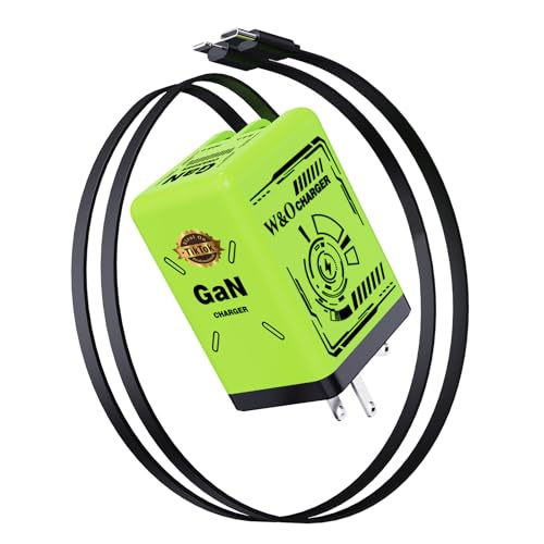
W & O 2-in-1 gan Compatible with Fast Charger,Retractable Phone Charger with Cables,45W iPhone Charger Fast Charging,Fast Charger for iPhone16/15/14/13 Series, Galaxy S25/24,Android and More(Green)
Retractable Travel Charger with Dual Cables:Our iPhone charger fast charging comes with Type-C and Lightning cables that extend…
As an affiliate, we earn on qualifying purchases.
As an affiliate, we earn on qualifying purchases.
The Basics of Gan Transistors and How They Differ From Traditional Silicon Devices

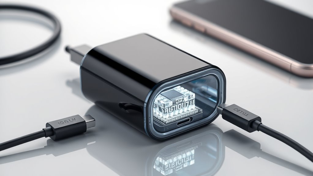
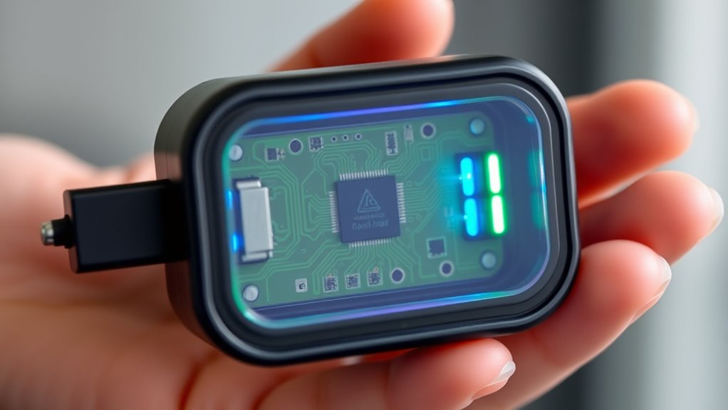
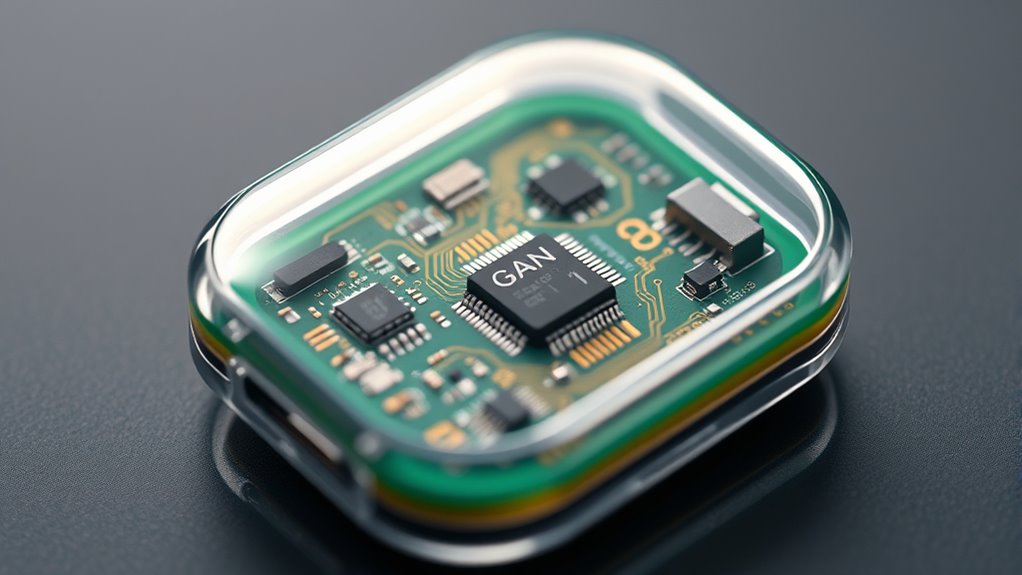
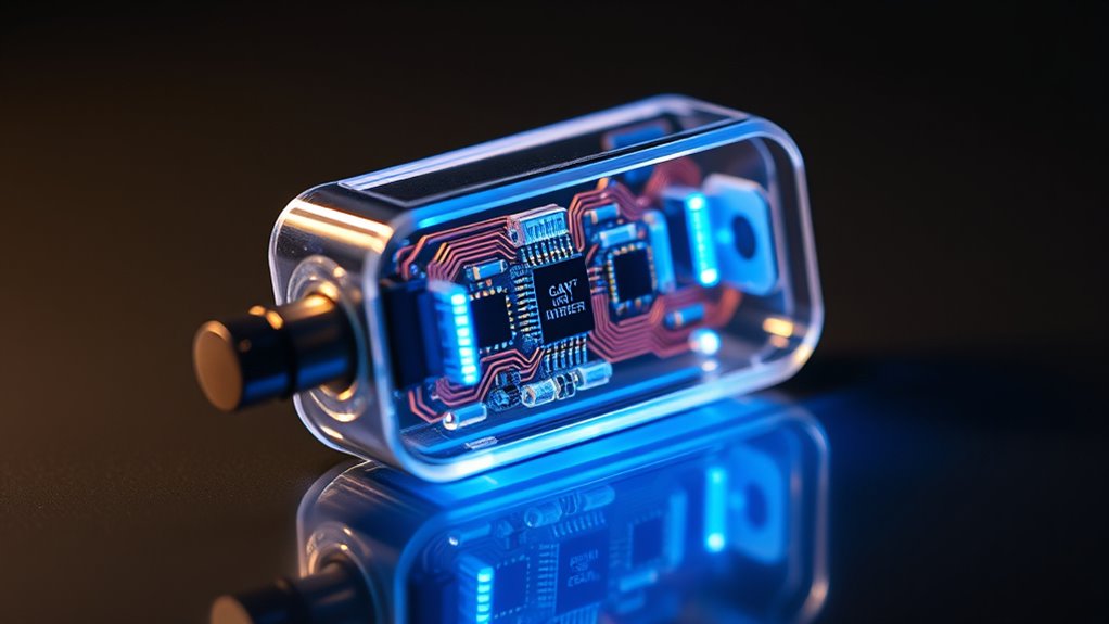
Gallium Nitride (GaN) transistors are revolutionizing power electronics by offering significant advantages over traditional silicon devices. Unlike silicon transistors, GaN transistors use a different semiconductor material that allows for faster switching speeds and higher efficiency. This means you can handle more power with less heat and smaller components. GaN devices operate at higher voltages and frequencies, reducing energy loss during operation. They are also more compact because they require fewer cooling measures and less space for heat dissipation. You’ll notice that GaN transistors turn on and off quicker, making them ideal for high-speed applications. Additionally, their thermal management capabilities help maintain optimal performance under demanding conditions. Overall, their unique properties give you a more efficient, smaller, and faster electronic system compared to conventional silicon-based devices.

UGREEN 3-Port 30W USB C Charger, GaN II Compact iPhone Charger Fast Charging, Type C Power Adapter for iPhone 17/16/15 Series, Galaxy S26/S25/24, iPad, MacBook, Matt Black
Faster & Cooler Choice: This UGREEN USB C Charger Block supports a max power transmission of 30W. Within…
As an affiliate, we earn on qualifying purchases.
As an affiliate, we earn on qualifying purchases.
Advantages of Using GaN in Power Conversion and Charging Applications
Using GaN in power conversion and charging lets you achieve higher efficiency and generate less heat. This means your devices can be smaller and lighter without sacrificing performance. Ultimately, GaN helps you design more compact and reliable chargers. Incorporating creative practice principles can also lead to innovative design solutions that further optimize device performance and form factor.
Higher Efficiency, Less Heat
Thanks to their superior electrical properties, GaN transistors deliver higher efficiency in power conversion and charging applications, which means less energy is lost as heat. This improved efficiency allows your chargers to convert more of the input power directly into usable energy, reducing waste. Less heat generation not only increases overall performance but also minimizes thermal management needs, making devices more reliable and longer-lasting. With less heat, components operate cooler, improving safety and reducing the risk of overheating. This efficiency gain also means your chargers can deliver faster charging speeds without sacrificing energy conservation. Ultimately, GaN transistors help you achieve more compact, powerful chargers that run cooler and more efficiently, enhancing your user experience and lowering energy consumption. Utilize vertical storage solutions to optimize space within your charging station or workspace.
Smaller, Lighter Devices
Building on the efficiency benefits of GaN transistors, they also enable the creation of smaller and lighter chargers. Because GaN switches faster and handles higher voltages in a compact form, engineers can design power supplies without bulky components. This means your chargers can be markedly reduced in size while maintaining strong performance. Lighter chargers are not only easier to carry but also generate less heat, reducing the need for heavy cooling solutions. As a result, you get a sleek, portable device that fits easily into bags or pockets. The miniaturization doesn’t compromise power; instead, it enhances convenience and usability. GaN technology empowers manufacturers to deliver powerful, compact chargers that match your on-the-go lifestyle, making charging quicker and more efficient everywhere you need it. High efficiency in power conversion ensures these chargers perform reliably over time while consuming less energy.

Nobsound 36V 6A Power Supply: 216W High-Efficiency GaN Adapter for Amplifiers, Active Speakers, LED Strip Lights, 3D Printers, AC 100-240V Input
216W GaN Tech – Efficient & Powerful: Using advanced GaN technology, this 36V/6A adapter minimizes energy loss and…
As an affiliate, we earn on qualifying purchases.
As an affiliate, we earn on qualifying purchases.
Design Innovations Enabled by GaN Transistors for Smaller Chargers
GaN transistors have revolutionized charger design by enabling significant reductions in size without sacrificing performance. They allow engineers to rethink traditional power supply layouts, integrating fewer components and reducing circuit complexity. With GaN, you can create smaller, more efficient power converters that fit into compact enclosures. These transistors operate at higher switching frequencies, which means you can use smaller inductors and capacitors, further shrinking the charger. Additionally, GaN’s thermal efficiency reduces the need for bulky heatsinks, saving space. This innovation also enables flexible PCB designs, optimizing space utilization. Moreover, the use of high-end materials in manufacturing GaN transistors enhances their durability and performance. Overall, GaN transistors push the boundaries of miniaturization, making it possible to develop chargers that are not only smaller but also more versatile, durable, and easier to manufacture.

Anker Prime Charger, 100W 3-Port GaN USB C Charger Block, Foldable and Compact for MacBook, iPad, iPhone 17 Series, Galaxy S24/S23, and More
100W Multi-Device Fast Charger: Power up three devices simultaneously with a total of 100W output through two USB-C…
As an affiliate, we earn on qualifying purchases.
As an affiliate, we earn on qualifying purchases.
Impact of GaN on Charging Speed and Efficiency
GaN transistors enable faster charging speeds by reducing resistance and allowing higher current flow. They also cut down on power losses, making chargers more efficient overall. As a result, you get quicker charge times in a smaller, more portable package.
Faster Charging Rates
Thanks to the superior electrical properties of GaN, chargers can deliver power at considerably higher rates without generating excessive heat. This means you can charge your devices faster than ever before, often reducing charging times by half or more. GaN transistors switch on and off more efficiently, allowing for rapid power transfer while maintaining stability. Their ability to handle higher voltages and currents without overheating enables compact chargers to push more power through smaller components. As a result, your devices can reach full charge quickly, saving you time. GaN’s efficiency guarantees that the increased charging speed doesn’t compromise safety or longevity. Additionally, the integration of GaN technology supports advanced automation in charger manufacturing, leading to more reliable and innovative designs. Overall, GaN technology transforms your charging experience by combining rapid power delivery with reliability, all within a smaller, more portable charger.
Reduced Power Losses
By reducing power losses during operation, GaN transistors make charging more efficient and faster. Traditional silicon transistors waste energy as heat, which limits how quickly and efficiently you can charge your devices. GaN transistors switch faster and operate at higher voltages with less energy loss. This means less heat is generated, and more power is delivered directly to your device. As a result, chargers using GaN technology can sustain higher power levels without overheating, boosting overall efficiency. You benefit from shorter charging times and improved energy use, making your charging experience more reliable and environmentally friendly. By minimizing wasted energy, GaN transistors optimize power transfer, ensuring your devices charge quickly while consuming less electricity.
Smaller Charger Size
Reduced power losses in GaN transistors not only improve charging efficiency but also enable chargers to become substantially smaller. Because GaN transistors handle higher voltages and currents more effectively, designers can shrink the size of the internal components. This means you get a compact charger without sacrificing performance. GaN’s efficiency reduces the need for bulky heat sinks and large capacitors, allowing for sleeker designs. You’ll notice your charger is lighter and more portable, perfect for travel or everyday use. The smaller size doesn’t compromise speed; it actually enhances fast charging capabilities. Overall, GaN technology lets you enjoy powerful, efficient charging in a much more convenient, space-saving package. Effective thermal management is also facilitated by GaN’s superior heat dissipation properties, further enabling compact design.
Challenges and Considerations in Implementing GaN Technology
Implementing GaN technology presents several challenges that manufacturers and designers must carefully navigate. One primary concern is managing heat since GaN devices operate at higher efficiencies but can still generate significant heat if not properly cooled. You also need to address material quality; ensuring consistent, defect-free GaN wafers is vital for reliability. Additionally, GaN transistors are more sensitive to voltage spikes and electrostatic discharge, requiring robust protection circuits. Designing compatible power delivery systems can be complex, as traditional components may not work efficiently with GaN’s fast switching capabilities. Cost considerations also play a role; although GaN devices offer long-term savings, initial expenses can be higher. To succeed, you must balance performance, safety, and cost, while carefully addressing these technical hurdles. Furthermore, the thermal management of GaN devices is crucial for maintaining optimal operation and preventing device failure.
Future Trends in Compact Charger Development With Gan Transistors
Advancements in GaN transistor technology are paving the way for increasingly compact and efficient chargers. Future developments will focus on integrating GaN devices into smaller form factors while boosting power density. You can expect chargers to become lighter, with higher charging speeds and improved thermal management. Innovations like multi-layer packaging and advanced circuit designs will reduce size without sacrificing performance. Smart features, such as adaptive charging and enhanced safety protocols, will become standard. Manufacturers will also explore using GaN in wireless and multi-port chargers, catering to diverse device needs. As GaN technology matures, costs will decrease, making high-performance chargers more accessible. Additionally, the reliability of GaN components will improve with ongoing research, ensuring longer-lasting products. Overall, these trends will enable you to enjoy faster, more portable charging options that fit seamlessly into your daily life.
Frequently Asked Questions
How Does Gan Impact Overall Device Reliability?
You might wonder how GaN transistors affect device reliability. GaN transistors are highly efficient and generate less heat, reducing thermal stress on components. This leads to longer device lifespan and fewer failures. Additionally, GaN’s robustness allows chargers to operate at higher frequencies and voltages without compromising reliability. Overall, integrating GaN transistors enhances your device’s durability and performance, making your charger more dependable over time.
Are Gan Chargers Compatible With All Electronic Devices?
GaN chargers are compatible with most electronic devices because they support common charging standards like USB-C and Power Delivery. You can safely use them to charge smartphones, tablets, and laptops. However, always check your device’s power requirements and the charger’s specifications to verify compatibility. While GaN chargers are versatile, some older or specialized gadgets might need specific power settings, so double-check before plugging in.
What Are the Cost Differences Between Gan and Silicon Chargers?
Considering cost differences, GaN chargers generally cost more upfront than silicon chargers, but they save you money long-term. You get smaller, faster, and more efficient charging in a compact package. While silicon chargers may seem cheaper initially, GaN tech’s efficiency means you’ll spend less on energy and replacement over time. So, your investment today pays off with performance, portability, and savings tomorrow.
How Does Gan Technology Affect Charger Manufacturing Processes?
GaN technology impacts charger manufacturing by allowing you to design smaller, more efficient components. It enables faster switching and reduces heat generation, so you can use fewer parts and simplify assembly. This streamlines your production process, cuts costs, and shortens development time. Overall, GaN transistors let you create more compact, reliable chargers, giving you a competitive edge in the fast-growing market for portable, high-performance power solutions.
Can Gan Transistors Be Integrated Into Existing Charger Designs Easily?
You can integrate GaN transistors into existing charger designs more easily than you might think. They’re compatible with standard manufacturing processes, allowing you to replace traditional silicon components without a complete redesign. GaN’s small size and high efficiency mean you can upgrade your chargers to be more compact and powerful without significant changes. This flexibility helps you keep up with technological advancements while maintaining cost-effectiveness in production.
Conclusion
By embracing GaN transistors, you open smaller, faster chargers that outshine traditional silicon devices in efficiency. While the compact size and rapid charging may seem like the ultimate goal, don’t overlook the challenges in manufacturing and integration. As GaN technology advances, you’ll find that the future of charging balances cutting-edge innovation with practical considerations—transforming your experience from bulky to sleek, and from slow to lightning-fast. The future is compact, powerful, and just a charge away.